



Europe is stepping up efforts to establish itself as a major player in the next generation of semiconductor technology, as investments in photonic chips raise hopes of transforming the global computing industry.
Ton van Mol of Dutch research institute TNO believes photonic chips are approaching a major technological breakthrough, a development that could create new opportunities for Europe to compete with established semiconductor leaders.
Unlike conventional computer chips, which process information using electrical signals, photonic chips rely on light to transmit and process data. The technology promises higher processing speeds, reduced energy consumption and less heat generation.
Traditional electronic chips power everything from smartphones and televisions to large data centres supporting the growing demand for artificial intelligence. Their operations depend on the movement of electrons through microscopic circuits containing billions of transistors.
Van Mol believes photonic technology could experience growth comparable to the rapid development of electronic semiconductors over the past five decades.
“With optical chips, you are now where electronic chips were maybe 40 [or] 50 years ago,” he said.
The emerging technology presents Europe with an opportunity to strengthen its position in an industry currently dominated by companies in the United States, Taiwan and China.
To support that ambition, the European Union has committed €400 million ($450 million; £330 million) to PIX Europe, an initiative designed to establish the continent as a global leader in photonic integrated chip technology.
Van Mol, who is coordinating a key component of the programme, said Europe recognised the importance of developing independent manufacturing capabilities rather than relying heavily on foreign suppliers.
He explained that the European Chips Act was introduced partly to strengthen the region’s semiconductor production capacity, including through pilot manufacturing facilities intended to move emerging technologies from research laboratories into industrial production.
Europe targets large-scale photonic chip production
One of the major challenges facing the industry is increasing manufacturing capacity and improving production efficiency.
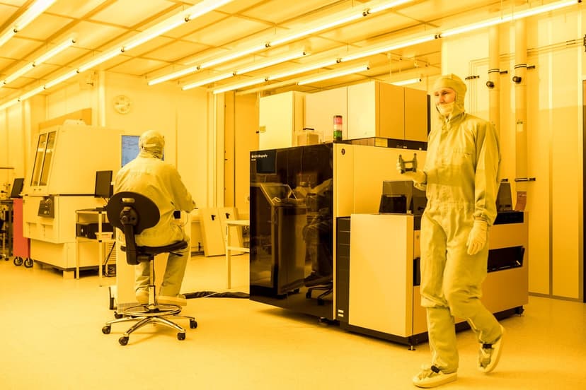
Photonic and electronic semiconductors are manufactured on silicon or other material wafers containing multiple individual chips. Larger wafers can allow manufacturers to produce more chips efficiently within a single production cycle.
According to Van Mol, most photonic chip manufacturing currently operates with four-inch (10cm) wafers, making the transition to six-inch wafers an important next step.
TNO is developing a 10,000-square-metre manufacturing facility at the High Tech Campus in Eindhoven, the Netherlands, where six-inch indium phosphide wafers will be produced.
The facility is expected to become fully operational in 2030, marking a significant development for photonic semiconductor manufacturing in Europe and potentially the wider global industry.
Van Mol said the project would establish a serious pilot production line capable of delivering consistent manufacturing results.
The objective is to achieve a stable, repeatable and high-yield production process by 2030, after which the facility is expected to accommodate industrial companies interested in commercial manufacturing.
ASML’s expertise strengthens Europe’s ambitions
Europe’s ambitions are supported by its existing semiconductor technology ecosystem, particularly the Netherlands-based equipment manufacturer ASML.
The company holds a unique position in the global semiconductor industry as the sole supplier of the advanced lithography machines used to manufacture the world’s most sophisticated chips.
ASML equipment is expected to play an important role in the Eindhoven pilot facility, which is located close to the company’s headquarters.
Van Mol noted that photonic chip manufacturing shares several similarities with conventional semiconductor production, including the use of wafers, specialised equipment and advanced cleanroom facilities.
ASML is also exploring the opportunities presented by photonics as the technology moves towards industrial-scale production.
Stanislas Baron, head of ASML’s EU/US Customer Team, said Europe had established a strong foundation in photonics research but needed to improve its ability to convert scientific breakthroughs into large-scale manufacturing.
The Netherlands has already benefited significantly from ASML’s success, which has helped develop a strong network of semiconductor companies, research institutions and technology specialists around Eindhoven.
European policymakers and industry leaders hope to replicate that model within the emerging photonics sector.
Former ASML chief executive Peter Wennink has also backed the initiative. His influential report for the Dutch government, The Roadmap to Future Prosperity, projected that the photonics market could expand by between 10 and 20 times over the following decade.
Describing the Eindhoven pilot facility as an important investment in Europe’s technological future, Wennink said expanding scalable manufacturing capacity would help establish an ecosystem capable of influencing the direction of global technology.
He characterised the initiative as “a launchpad for Europe’s future digital economy”.